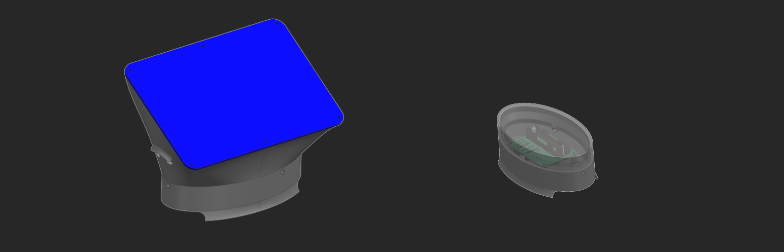
The project goal was to design, implement, and fabricate a sensor node for monitoring outdoor air quality by measuring particulate matter, volatile organic compounds (VOCs), volatile sulfuric compounds (VSCs), temperature, and pressure. The device needed to run on battery power and support charging via photovoltaic cells to keep the node operating in remote locations. The device operating environment was defined as Finland and Germany, around the year.
The files for this board can be found at GitHub.
Requirements
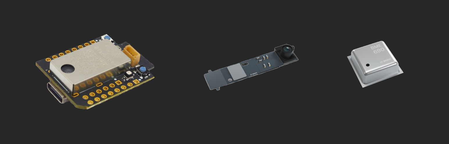
Initially the project was designed around Black IoTs Polverine board, which is specifically designed for environmental sensing. The Polverine uses an ESP32-S3 and has BME690 (VOCs, VSCs, T, Rh, P) and BMV080 (PM2.5) onboard the MCU module; however, at halfway point the hardware requirements changed. The BMV080 had a specified ambient operating range between 15-65°C, which meant it couldn’t be used reliably outside during winter in Finland. This was the point where the project split to support two configurations.
The first configuration is based around the Polverine board and uses Bosch BME690 (SPI) and Bosch BMV080 (I2C) for sensing. The second configuration is based around a DFR1117 (ESP32-C6) board, and uses Sensirion SPS30 (PM2.5, I2C) and TC74A2 (T, I2C) for sensing. In both configurations data is sent to the backend using a Seeed Studio LoRa-E5 (UART).
More specific electrical details or requirements weren’t really defined at any point –despite a lot of pestering on my part. The general gist was simply to have a battery, support for photovoltaic charging, appropriate power rails, and connectors for our MCU module and the used peripherals. There wasn’t a specified requirement for how long the device should operate on battery power.
Power
Both the Polverine and DFR1117 can be powered using 5V, and provide 3V3 outputs via an exposed pin from their onboard LDOs (TLV75733P and TPS62A02DRLR respectively). From the peripherals only the SPS30 required 5V to operate, all else could run off 3V3.
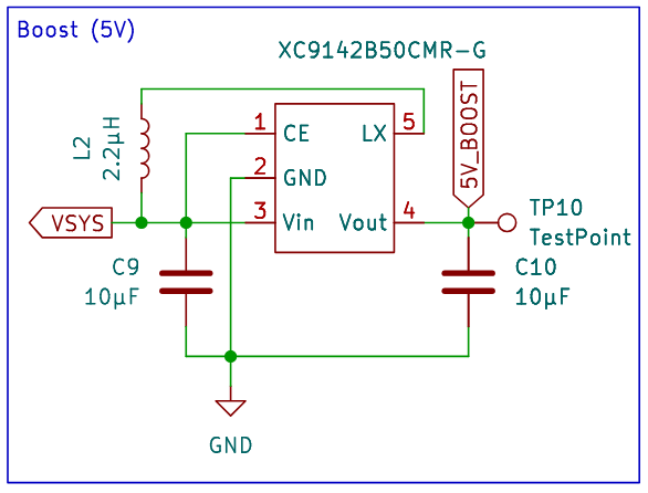
I decided to use a boost switching regulator (XC9142V50CMR-G) to get a stable 5V output that could power the MCU modules and the SPS30. All other 3V3 peripherals would then run off the MCU LDOs. The boost would be fed from either the battery or one of the optional external power inputs (stabilised solar, USB-C, or pin-header).
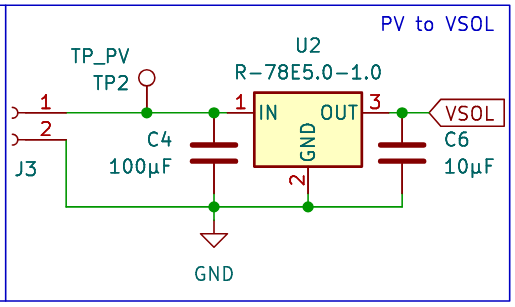
Choosing a way to regulate the Solar output depended on the used panel. For a lower voltage IoT photovoltaic panel an LDO would be a better choice, but as the panel I had was generic and had a relatively high voltage of 24V I opted to use the switching regulator from Recom (R78E-1.0, 8-28Vin) that outputs a stable 5V. I could then combine this output with the other external inputs like the USB-C and pin-header by using schottky diodes to get a combined 5V external power rail.
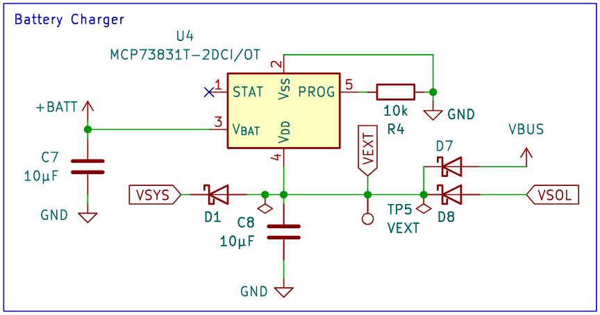
The external power rail would feed the battery charger (MCP73831T-2DCI/OT), which had a maximum input voltage of 6V. The external power rail is further combined with the battery output that feeds the 5V boost. Small voltage drops due to the schottky diodes along the path making sure the voltage stays within an acceptable span at the boost input, even if some external power input slightly exceeds its specified maximum output (E.g. USB-C port at ~5.25V).
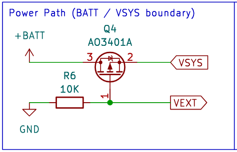
The external power rail also actuates the P-FET gate separating battery from the system load when sufficient voltage is present to charge and drive the load via an external power source. When the draw exceeds what is required, the voltage naturally collapses and the battery is automatically reconnected to the system as the FET gate is pulled to ground.
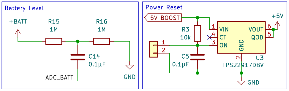
The battery is defined to be a LiPo with 3.6V nominal voltage and range of [2.4V,4.2V]. It is protected from overvoltage, undervoltage, overcharge, overdischarge by a DW01 IC that uses a dual N-FET to disconnect the battery ground from system ground when any of the aforementioned conditions are met. The battery positive track has a voltage divider with 1M Ohm resistors for a voltage divider with a 0.1µF capacitor to allow reading the current battery voltage via an ADC pin on the used MCUs in the range of 0% (1.2V), 100% (2.1V).
I also added a power switch (TPS22917DBV) that allows flushing the main 5V power rail to perform a full system and peripheral reset. This wasn’t a specified requirement, but I felt it was a rather obvious inclusion as a reset pin wasn’t exposed on both the Polverine and DFR1117. Having the reset switch built into the PCB makes sure the MCU and all peripherals reset and functionality stays consistent between the configurations.
Peripherals
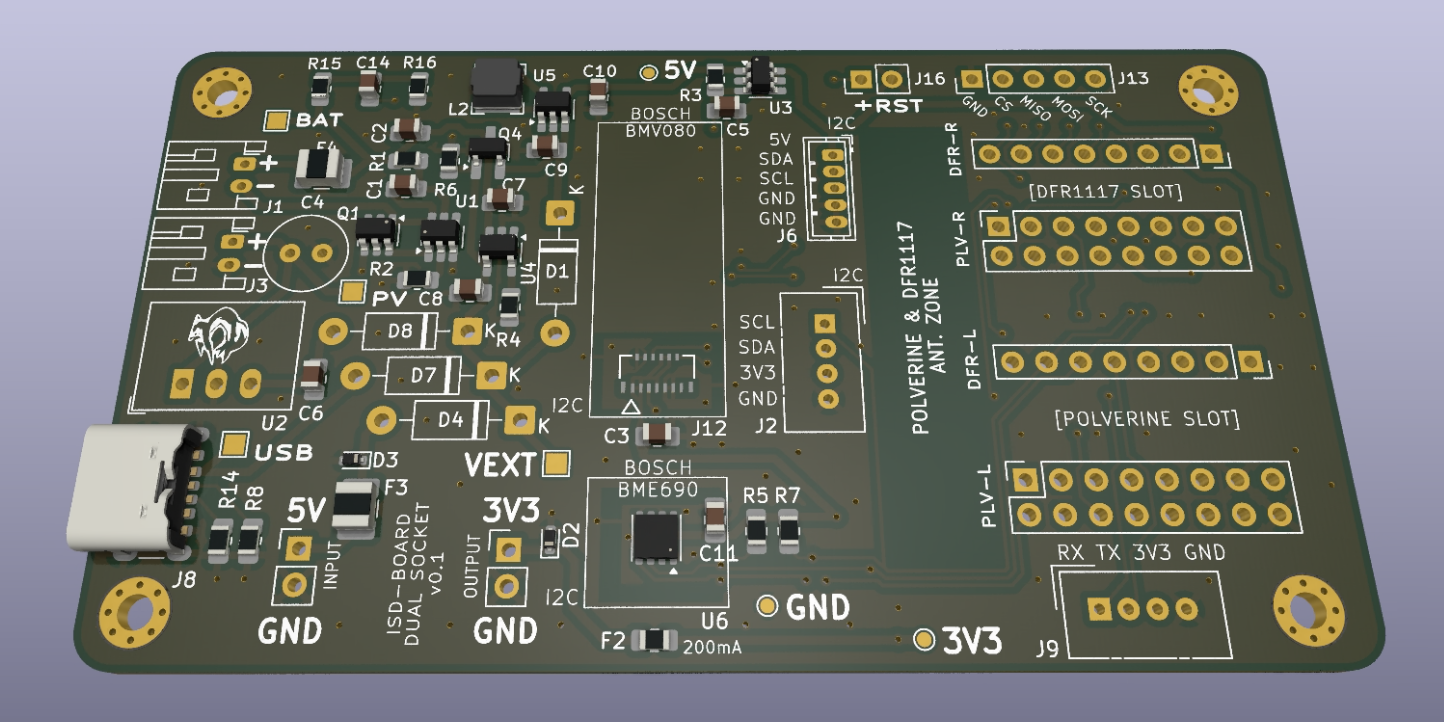
First configuration relies on the Polverine and its onboard sensors (BMV080, BME690), and only requires a Grove connector (UART, 3V3) for the E5 LoRa module for connectivity.
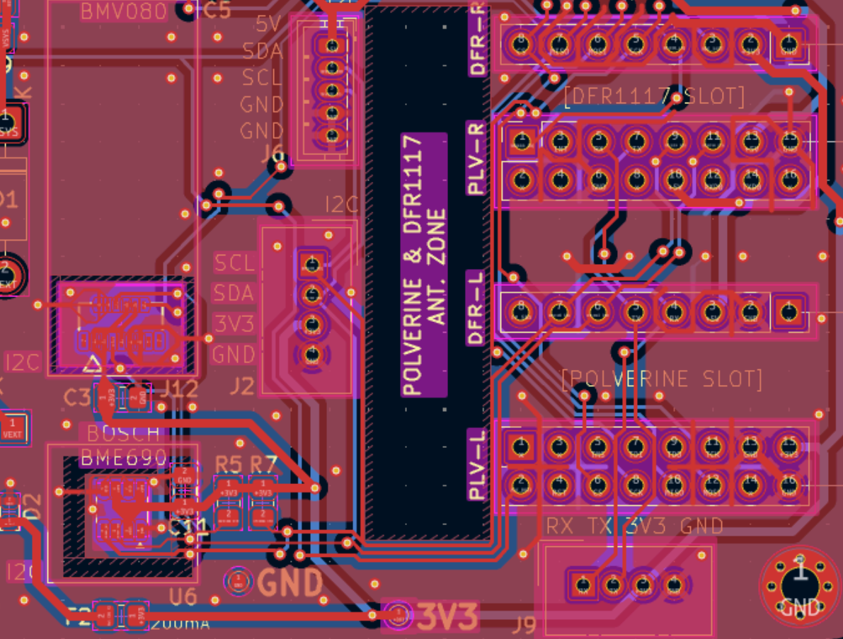
Second configuration on the other hand uses the PCB connectors for all sensors, and uses two Grove connectors and one ZHR-5. One Grove connector is used for the E5 LoRa module and the other for TC74A2 (I2C, 3V3). The ZHR-5 is used for the SPS30 (I2C, 5V). As a bonus, we decided to add footprints for integrating the BME690 (LGA) and BMV080 (ZIF) directly onto the PCB so using them would be possible with the DFR1117 as well. I modified the LGA pad slightly by extending the pads out from underneath the package so it could be hand-soldered with an iron.
I also added two optional pull-up resistors for the I2C signal lines (R5, R7).
Fabrication and Assembly
The PCBs were ordered from JLCPCB as regular 2-layer FR4 boards. I chose not to use any lead. They had a coupon (shocker) for stencils, so I grabbed those as well. I think in the future I’ll try PCBway, as their prices seem cheaper for the most affordable shipping options. This time the deadline meant I couldn’t wait around for the boards to arrive by camel.
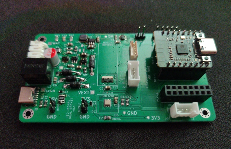
I hand-assembled the boards with an iron and some unleaded solder. I used a bit of flux for the multi-pin ICs, and had a certain kind wizard solder the LGA and ZIF connector by hand.
It’s not the prettiest job on my part, but the compononents are on!
Integration Testing & Validation
Finland
The project integration testing and presentation was scheduled for 2026.02.26-27, in Osnabrück (Germany). I hurried to assemble the board the previous night before leaving there and finished at around 4am. In the morning I had barely time to validated the following basics to be fully functional:
- External Power Inputs
- USB-C
- Photovoltaic (Lab PSU, 8-25V range)
- Pin header (Lab PSU, 4.2-5.1V range)
- System and Peripheral Rails
- Main 5V power rail (Boost)
- Peripheral power rails (5V, and MCU LDO at 3V3)
- MCU Sockets
- DFR1117 blinky was OK.
- Power switch
- Was functional and flushed the main power rail cleanly, resetting device and peripherals.
- Charging IC
- Prog pin was at 1V when receiving sufficient voltage, as described in the datasheet.
- Voltage Divider
- Seemed to be functional, but due to the high resistance used I was unable to get the exact value on my multimeter, and I didn’t have the code to test on the DFR1117.
I couldn’t validate the battery input or power path FET functionality fully, as the FET part I received wasn’t what I had specified in the Bill of Materials (BOM). Only later in Germany did I realise the part could be soldered at an offset to have the pins reach correct pads, despite the physical package and pin mismatch. I bent the unneeded pins above the package to avoid shorts due to the unconventional mounting.
Germany
Most of the time in Germany by me was spent helping the sensor and LoRa teams with integration. Things like explaining that the PCB needs to power the 5V peripheral bus (so they couldn’t just power the MCU via its USB-C), fixing badly soldered and janky cabling or pin-headers that the teams had cobbled together –they interfered with results in testing. I had the foresight to print out a few schematics, routing planes, and BOMs to help the teams understand where everything was connected (Link). I certainly had a much better experience using the physical paper than lugging a laptop between different stations.
I only had made two prototypes, and gave one to each MCU team (sensor and LoRa). They seemed to enjoy being able to plug everything into a single PCB and ditch their breadboard solutions when it was all working. The downside to this was that I was then left without a board to validate and solve the rest of the issues on…
The only real issues that got into the way during this testing was the DW01A protection IC, and the ZIF-connector.
The ZIC-connector issue is very simple. I misread the datasheet and thought the front-row was the back-row and vice versa. This means that the physical latch on the connector is rotated 180deg from the expected direction, and the pin numbering is flipped relative to insertion direction… Yeah… Sadly there is no interesting technical problem to be solved, other than to have more people sign off on parts that are sufficiently questionable in the future. To be fair, I did ask multiple people, and no one caught it; though, I’m sure I could’ve made my request more systematic to have better chances of catching this. As the connector is such a fine-pitch, there is no real way to have a workaround. Luckily this was just a bonus connector, so it didn’t affect either of the two desired configurations.
The more pressing issue was the DW01A, which seemed to freak out the moment a battery was plugged into a system that was off. There were two solutions employed during the integration testing.
One was to simply bypass the protection circuit with a jump wire between battery ground and system ground (bypass the mosfet, and thus DW01A protection). This forfeits the protections afforded by the IC, and is less than optimal, but at least the charging IC has overcharging protections, so the system practically loses just the lower limit protections which isn’t really an issue for a short demo.
The second solution was frankly quite dumb, and was discovered with an oscilloscope by monitoring the PROG pin on the DW01A. It appeared to rise fast to 3.6V (Batt voltage) when initially connected, which was higher than expected. It would then crash down exponentially to 0V. It was hypothesised that this quick change and its magnitude was triggering the protections and immediately disconnecting the battery upon insertion. As to why this would trigger the protection is unknown (time constraints), and seems quite nonsensical. Either way, this wouldn’t happen if the system was powered from an external power source first, like the USB-C or Solar panel, and the battery was then plugged into an already running system. It was then possible to unplug external power and the system would happily run from battery or external power when appropriate by the power path management.
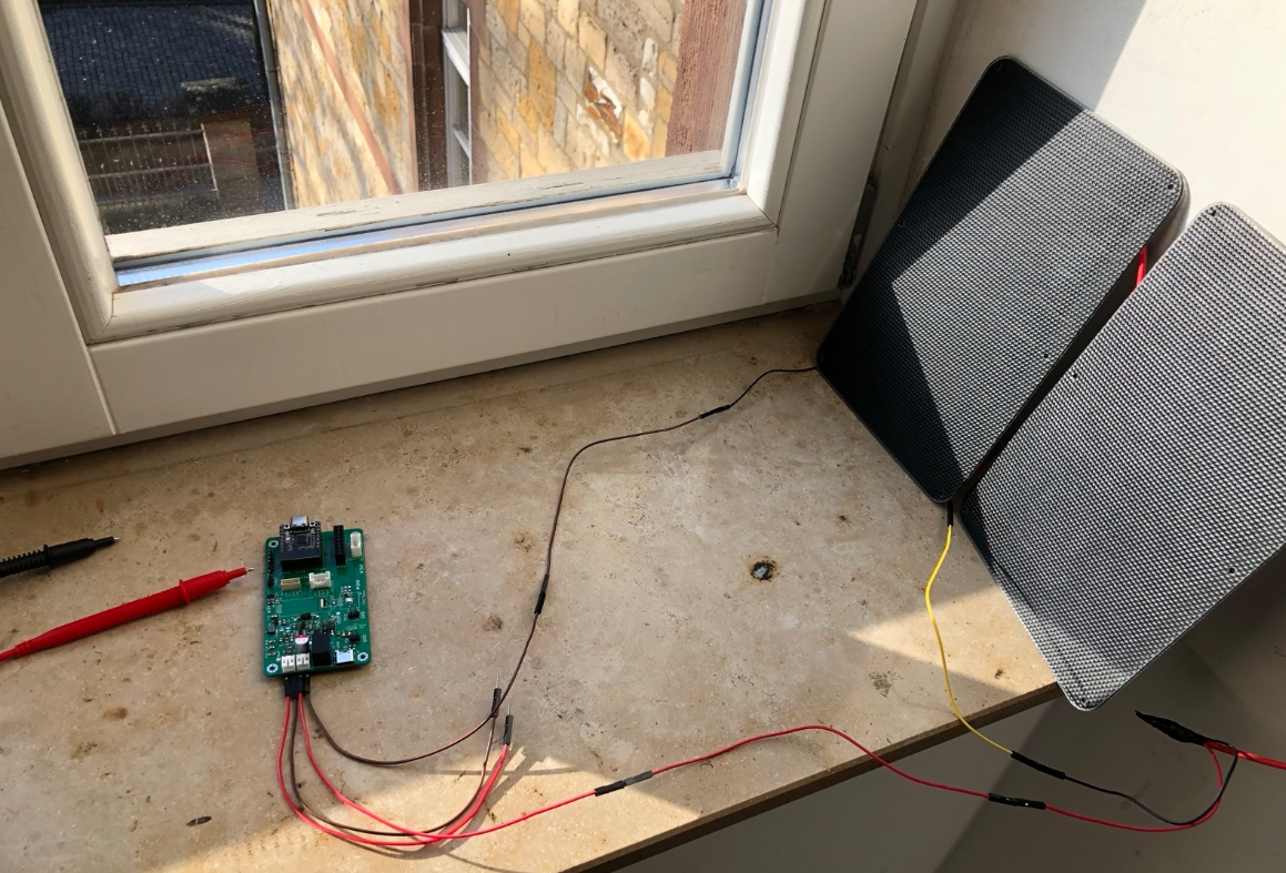
Moving onto things that did work, I also had the time to make sure it actually runs from a solar panel. Unfortunately I forgot to take the largest component (the solar panel) with me to Germany, so I had to use two of the lower voltage (~5V) panels that were available. I just spliced them in series to get 10V, and successfully powered the MCU with blinky code at the windowsill.
Conclusion
The presentation and PCB-demo was successful. The demonstrated PCB unit was stuffed into the mechanical enclosure within the last 15 minutes before the presentation started. The actual software was being flashed to the node during the time other teams were presenting. We were lucky the electronics team’s slides were the last ones!
I would definitely do a lot things differently if I were to start from scratch, and the list of things I’ve learned is more than a little lengthy. I don’t feel like listing all the lessons here, so I’ll just end by saying that I’ll use the gained experience for an upcoming IoT project. Most likely in the form of a more streamlined power module design that is reusable accross projects.
Sincere thanks to all the team members I worked with, the other project teams, and all the people who helped me during this project with everything!